ATI Radeon HD 5870 Performance
Still, there are people using the ATI Radeon HD 5870 today. Is it still good in 2021? We will see.
All warfare is based on deception. Hence, when able to attack, we must seem unable; when using our forces, we must seem inactive; when we are near, we must make the enemy believe we are far away; when far away, we must make him believe we are near. Hold out baits to entice the enemy. Feign disorder, and crush him.
– Sun Tzu, The Art of War
If your enemy is secure at all points, be prepared for him. If he is in superior strength, evade him. If your opponent is temperamental, seek to irritate him. Pretend to be weak, that he may grow arrogant. If he is taking his ease, give him no rest. If his forces are united, separate them. If sovereign and subject are in accord, put division between them. Attack him where he is unprepared, appear where you are not expected.
– Sun Tzu, The Art of War
These quotes, lifted from The Art of War — ancient Chinese text written by Chinese general Sun Tzu thousands of years ago yet still required reading for military theorists and some business schools — aptly describe ATI’s cunning gambit with Radeon HD 4000 series more than a decade ago in 2009.
Just when everyone was counting ATI out of the high-end graphics space, NVIDIA included, they delivered a homerun product with the Radeon 4850 and Radeon 4870 that stunned the world. You could make an argument that the ramifications were perhaps as significant as ATI’s first DirectX 9 product, R300 (Radeon 9700) was over fifteen years ago.
Think about it. As any hardware enthusiast who’s followed the industry can tell you, before the Radeon 4800 series cards arrived on the scene, graphics card prices were going nowhere but up. While it may seem hard to believe now, NVIDIA’s GeForce GTX 280 launched just two weeks before the Radeon 4870 at a staggering price tag of $649 MSRP. Its less powerful sibling, the GeForce GTX 260 carried an MSRP of $399.
That’s a steep climb up from the days when 3dfx’s original Voodoo Graphics card sold for $300. NVIDIA’s prior products, the GeForce 8800 Ultra and GeForce 8800 GTX sold for $829 and $599 respectively on their launch day.
Now before you think we’re out to get NVIDIA, they did give the mainstream segment one gem of a product in the form of the GeForce 8800 GT, and we said so when it debuted back in October of 2007: just in time for Crysis. What ATI pulled off with the Radeon 4800 series though was even more significant than the debut of the 8800 GT.
If you rewind back to the days in early 2008 ahead of the Radeon 4800 and GeForce GTX 200’s debut, you’ll remember that all the early rumors indicated that the Radeon 4850 would fall somewhere between the 8800 GT and 9800 GTX in performance, with pricing similar to the 8800 GT, while the Radeon 4870 would outperform 9800 GTX.
If you’re NVIDIA and you know you’ve got a performance behemoth like GT200 right around the corner, you’d be feeling pretty good about yourself and how your upcoming product will fare against your competitors. Some ATI fanboys were already blaming AMD for the supposed “death” of ATI’s high-end graphics and were ready to queue up Taps.
Ultimately, what ATI ended up delivering with the Radeon 4850 and 4870 was completely different in a good way. Priced at $200 (the same price NVIDIA’s 8800 GT sold for at the time), the Radeon 4850 delivered performance that was greater than the 9800 GTX, forcing NVIDIA to concoct the 9800 GTX+ as a counter to the 4850. Meanwhile, the Radeon 4870 had its sights set on the GTX 260, yet it was priced $100 less. NVIDIA was forced to counter this GPU with GTX 260 price cuts and rebate checks for early adopters who picked up GTX 260 and 280 cards ahead of the arrival of the new Radeons.
To this day the 216-shader GeForce GTX 260 and Radeon 4870 1GB are still cutthroat competitors.
ATI’s “sweet spot” strategy of delivering smaller, more cost effective gaming GPUs for the performance segment and then scaling that tech up and down for the high-end and value markets was a real game changer for the industry, and their execution on this strategy was executed as if it was masterminded by Sun Tzu himself.
Enough about the past though. Now its time for the dawn of a new era of DirectX 11 gaming. Given the success of their Radeon 4800 series, ATI wouldn’t have the benefit of surprise this time around. Instead they’re essentially using lessons learned with GDDR5 memory, the development of DirectX 10.1 hardware, and TSMC’s 40-nm manufacturing process to give them a time to market advantage over the competition,
Being first to market didn’t help Sega’s Dreamcast, but it’s worked wonders for Microsoft’s Xbox 360 (I know, it’s a terrible analogy that oversimplifies things, but it’s the first gaming-related comparison I could come up with). Which scenario will ATI’s next-generation Radeon 5870 ultimately end up? We can’t answer that question today, but we can tell you how it looks and performs with today’s games…not to mention its breakthroughs in noise and power consumption…and don’t forget the OC’ing. Read on for the full details!
The specs
If the RV770 GPU inside the Radeon 4850 and Radeon 4870 was ATI’s first TeraScale graphics engine (an obvious nod to the GPU’s distinction as the first desktop graphics card to break the 1 TeraFLOP mark), then RV870’s TeraScale 2 has to be twice as good right? Right. In fact, Radeon 5870 more than doubles the compute power of Radeon 4870 (1.2 TeraFLOPS), boasting up to 2.72 TeraFLOPS:
Radeon 5870 Specifications
TeraScale 2 Unified Processing Architecture
1600 Stream Processing Units
80 Texture Units
128 Z/Stencil ROP Units
32 Color ROP Units
GDDR5 interface with 153.6 GB/sec of memory bandwidth
PCI Express 2.1 x16 bus interface
DirectX 11 support
Shader Model 5.0
DirectCompute 11
Programmable hardware tessellation unit
Accelerated multi-threading
HDR texture compression
Order-independent transparency
OpenGL 3.2 support
Image quality enhancement technology
Up to 24x multi-sample and super-sample anti-aliasing modes
Adaptive anti-aliasing
16x angle independent anisotropic texture filtering
128-bit floating point HDR rendering
ATI Eyefinity multi-display technology
Three independent display controllers drive three displays simultaneously with independent resolutions, refresh rates, color controls, and video overlays
Display grouping: Combine multiple displays to behave like a single large display
ATI Stream acceleration technology
OpenCL 1.0 compliant
DirectCompute 11
Double precision floating point processing support
Accelerated video encoding, transcoding, and upscaling
ATI CrossFireX™ multi-GPU technology
Dual, triple, and quad GPU scaling
Dual-channel bridge interconnect
ATI Avivo HD Video & Display technology
UVD 2 dedicated video playback accelerator
Advanced post-processing and scaling8
Dynamic contrast enhancement and color correction
Brighter whites processing (blue stretch)
Independent video gamma control
Dynamic video range control
Support for H.264, VC-1, and MPEG-2
Dual-stream 1080p playback support
DXVA 1.0 & 2.0 support
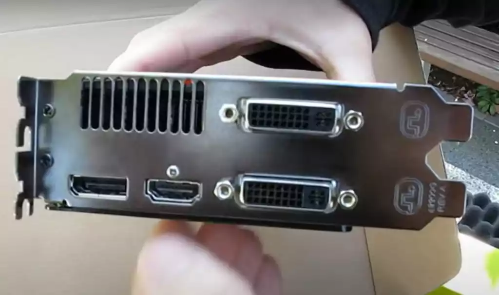
Integrated dual-link DVI output with HDCP (Max resolution: 2560×1600)
Integrated DisplayPort output (Max resolution: 2560×1600)
Integrated HDMI 1.3 output with Deep Color, xvYCC wide gamut support, and high bit-rate audio (Max resolution: 1920×1200)
Integrated VGA output (Max resolution: 2048×1536)
Integrated HD audio controller
Output protected high bit rate 7.1 channel surround sound over HDMI with no additional cables required
Supports AC-3, AAC, Dolby TrueHD and DTS Master Audio formats
Speeds and feeds
Engine clock speed: 850 MHz
Processing power (single precision): 2.72 TeraFLOPS
Processing power (double precision): 544 GigaFLOPS
Polygon throughput: 850M polygons/sec
Data fetch rate (32-bit): 272 billion fetches/sec
Texel fill rate (bilinear filtered): 68 Gigatexels/sec
Pixel fill rate: 27.2 Gigapixels/sec
Anti-aliased pixel fill rate: 108.8 Gigasamples/sec
Memory clock speed: 1.2 GHz
Memory data rate: 4.8 Gbps
Memory bandwidth: 153.6 GB/sec
Maximum board power: 188 Watts
Idle board power: 27 Watts
2.15 billion transistors w/334mm2 die size
40-nm manufacturing process
256-bit GDDR5 memory interface
500 Watt or greater power supply with two 6-pin PCI Express® power connectors
recommended (600 Watt and four 6-pin connectors for ATI CrossFireX™ technology in
dual mode)
RV870 Architecture
| RV770-RV870 Comparison | |||
| ATI Radeon HD 4870 | ATI Radeon HD 5870 | Difference | |
| Die Size | 263 mm2 | 334 mm2 | 1.27x |
| # of Transistors | 956 million | 2.15 billion | 2.25x |
| Memory Bandwidth | 115GB/sec | 153GB/sec | 1.33x |
| AA Resolve | 64 | 128 | 2x |
| Z/Stencil | 64 | 128 | 2x |
| # of Texture Units | 40 | 80 | 2x |
| # of Shaders | 800 | 1600 | 2x |
| Board Power | 90W idle, 160W load | 27W idle, 188W max | 0.3x, 1.17x |
If there’s only one key word to take away from the architecture of the new RV870 chip found inside ATI’s Radeon 5800 series cards it’s “2X”. Thanks to the smaller 40-nm manufacturing process, ATI can afford to double up on pretty much everything that made RV770 so special a year ago without having to charge double the price.
As you just saw on the specs page, RV870 boasts twice the SIMD units as its predecessor, RV770. Each SIMD unit consists of 80 stream processors and one texture unit, so with twice the SIMD cores, you’ve got twice the number of stream processors (1600) and twice the number of texture units, 20 (80 effective). Now ATI and NVIDIA use different nomenclature for what they both describe as a “stream processor” — the actual physical number of stream processing units inside RV870 is actually 320 — but regardless of the term you use to describe them, it’s an impressive amount of compute power nonetheless, as the 5870’s 2.72 TeraFLOPS can attest to.
The overall layout of RV870 is similar to RV770, just bigger. See for yourself in this RV870 block diagram:
The 20 SIMD cores are depicted as the red squares in the center of the diagram. If you look a little closer, you can sit and count the individual stream processing units for yourself. Like RV770 each stream processing unit consists of 4 stream cores+1 special function stream core which are tied to a branch unit and general purpose registers. ATI has tweaked them to improve their IPC.
Tied to each SIMD core is its own dedicated texture unit, again, just like RV770. RV870 boasts improved texel fill rate, up to 68 (bilinear filtered) Gigatexels/sec and improved data fetch rate: up to 272 billion fetches/sec. ATI’s also improved the cache bandwidth of the L1 texture caches tied to the texture units. RV870 sports up to 1 TB/sec L1 texture fetch bandwidth, while peak bandwidth between the L1 and L2 caches tops out at up to 435GB/sec.
In comparison, RV770 featured up to 480GB/sec of L1 texture fetch bandwidth and up to 384GB/sec of bandwidth between the L1 and L2 caches.
Up at the top of the block diagram, you’ll notice another significant tweak ATI has made with RV870 is the addition of a second rasterizer in the graphics engine of the chip. With a second rasterizer, RV870 feeds more pixels into the engine than its predecessor; this is important when you’re dealing with a GPU that’s outfitted with 1600 stream processors. ATI’s also updated their tessellator for DirectX 11 compliance.
256-bit memory interface
Moving to the bottom of the block diagram, you’ll also see RV870’s four 64-bit memory controllers, just like RV770. This probably comes as a bit of a disappointment to those of you who were hoping for a wider memory interface and the potential performance boost it could bring under high resolution, high AA scenarios (especially since some of the rumor sites were saying earlier this summer that RV870 would possess a wider memory interface), but in speaking with ATI, they felt that a 256-bit interface with high-speed GDDR5 was the way to go given their die size and transistor budget constraints.
Obviously implementing a wider interface is going to drive those demands up, which would’ve required ATI’s engineers to give up some of RV870’s 20 SIMD cores to compensate and remain on budget. It’s a tradeoff you have to make: integrate more stream processors or go wider with a larger interface? Given the lessons learned with R600’s 512-bit memory interface (where ATI basically couldn’t tap into all the bandwidth the larger interface provided and decided to go back to 256-bit for RV670), ATI decided to stick with a 256-bit memory interface and instead integrate more SIMD cores.
The way ATI sees it, GDDR5 data rates (i.e. clock speeds) are constantly improving while GDDR5 prices continue to go down. This is a more cost effective solution to the problem than implementing a larger memory interface.
ATI has made tweaks to their memory interface for RV870 though. To ensure data is transferred without errors, the controller can perform CRC checks on data transfers. ATI says this offers improved reliability at high clock speeds. The L2 cache size has been doubled to 128KB per memory controller. ATI also says GDDR5 memory clock temperature compensation enables speeds approach 5Gbps.
Power management
Besides is smaller manufacturing process, which naturally helps to reduce the GPU’s power consumption, ATI’s also integrated tweaks to further reduce RV870’s power consumption. As listed on the specs on the previous page, the chip consumes as little as 27W at idle. Impressive for a GPU to contains over 2 billion transistors.
A new low power strobe mode has been added to reduce memory power consumption, while ATI’s aggressive at reducing clock speeds and voltages at idle. At idle, Radeon 5870 runs at just 400MHz core/1200MHz memory.
For CrossFire users, ATI has also added a new ultra low power state for multi-GPU configurations that comes closer to shutting the secondary GPU(s) down when not in use. The second card throttles down to just 157MHz core/300MHz memory.
Recommended Articles
Our audience is interested in high-end devices, such as headphones with detachable cables, because you would not be losing sound quality with them.
We discuss the dirty screen effect and how to solve it. We explain to you why do we think that actually manufacturers are not really interested in solving this issue.
We explain how to choose projection screen material, for DYI projects and for large events where you would not find large projection screens in retail stores.
We have reviewed many receivers. Our recommended articles are our review of the Marantz SR7009 and the Onkyo TX-RZ820.
We have not reviewed many smart TVs. From those, however, in terms of price efficiency, I would like to recommend the Hisense B7500UW.
My favorite bookshelf loudspeaker is the Wilson Audio TuneTot and therefore we hope you like that review. We have also compared the Elac B5 vs the Elac B6, and do not think that the B6 is necessarily better in all the specifications compared.
In regard to connectivity and cable management, we discuss the connection between Firewire and HDMI.

I am Chris, a musician. I work as an audio engineer in mastering and arranging bridges in existing songs and the arrangement and orchestration of chorus. In Firing Squad I test gear provided by local distributors during a couple of days and write a review. I also write about AV topics, amplifiers, speakers and headphones.
Author And Fact Check
Written by author J. Bond and fact checked by Martin Pino and J. Esposito to ensure that the data retrieved is objectively correct